3. Información sobre la tarjeta DE10-Lite
3.1. Circuitería del reloj
La Figura 3.1 muestra la frecuencia predeterminada de todos los relojes externos a la FPGA MAX 10. Se utiliza un generador de reloj para distribuir señales de reloj con bajo jitter. Los dos relojes de 50MHz conectados a la FPGA se utilizan como fuentes de reloj para la lógica del usuario. Se conecta una señal de reloj de 24 MHz a las entradas de reloj del microcontrolador USB del USB Blaster. Una señal de reloj de 10MHz está conectada al PLL1 y PLL3 de la FPGA, las salidas de estos dos PLL pueden conectarse el reloj ADC. La asignación de pines asociada para las entradas de reloj a los pines de E/S de la FPGA se listan en la Tabla 3.1.
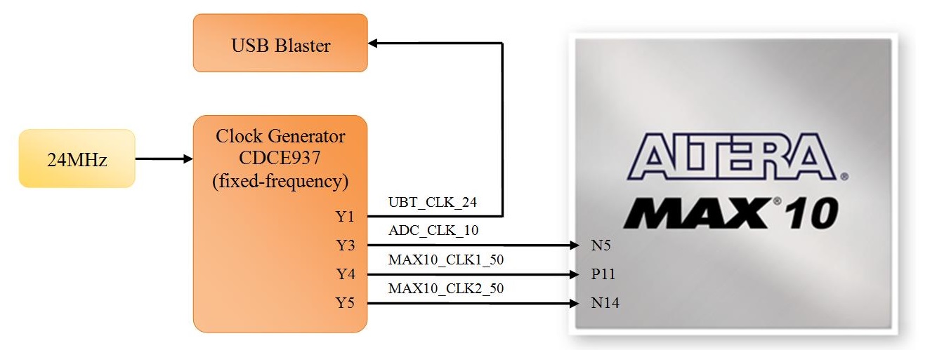
Figura 3.1 Circutiería de reloj en la tarjeta DE10_lite
Signal Name |
FPGA Pin No. |
Description |
I/O Standard |
|---|---|---|---|
ADC_CLK_10 |
PIN_N5 |
10 MHz clock input for ADC (Bank 3B) |
3.3-V LVTTL |
MAX10_CLK1_50 |
PIN_P11 |
50 MHz clock input(Bank 3B) |
3.3-V LVTTL |
MAX10_CLK2_50 |
PIN_N14 |
50 MHz clock input(Bank 3B) |
3.3-V LVTTL |
3.2. Uso de los Push-buttons, Switches y LEDs
3.2.1. Pulsadores (Push-buttons) definidos por el usuario
La tarjeta incluye dos pulsadores definidos por el usuario que permiten a los usuarios interactuar con el Dispositivo MAX 10 FPGA. Cada uno de estos interruptores es antirrebote utilizando un circuito de disparo Schmitt como se indica en la Figura 3.2. Una función de disparo Schmitt introduce histéresis a la señal de entrada para mejorar la inmunidad al ruido, especialmente para señales con transiciones de flanco lentas y actua como interruptor antirrebote (debouncer) en la Figura 3.3 para los pulsadores conectados.
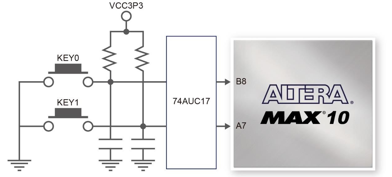
Figura 3.2 Conexión de los pulsadores y la FPGA MAX 10
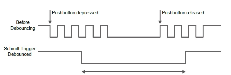
Figura 3.3 Efecto del antirrebote en los pulsadores
Signal Name |
FPGA Pin No. |
Description |
I/O Standard |
|---|---|---|---|
KEY0 |
PIN_B8 |
Push-button[0] |
3.3 V SCHMITT TRIGGER |
KEY1 |
PIN_A7 |
Push-button[1] |
3.3 V SCHMITT TRIGGER |
3.2.2. Interruptores (Switch) definidos por el usuario
Hay diez interruptores deslizantes conectados a FPGA en la placa (Ver Figura 3.3). Estos interruptores son utilizados como entradas de datos en un circuito. Cada interruptor está conectado directa e individualmente a un pin en el MAX 10 FPGA. Cuando el interruptor está en la posición ABAJO (más cercano al borde de la placa), proporciona un nivel lógico bajo a la FPGA, y cuando el interruptor está en la posición ARRIBA, proporciona un alto nivel lógico.
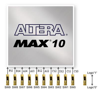
Figura 3.4 Conexión de los interruptores y la FPGA MAX 10
Signal Name |
FPGA Pin No. |
Description |
I/O Standard |
|---|---|---|---|
SW0 |
PIN_C10 |
Slide Switch[0] |
3.3-V LVTTL |
SW1 |
PIN_C11 |
Slide Switch[1] |
3.3-V LVTTL |
SW2 |
PIN_D12 |
Slide Switch[2] |
3.3-V LVTTL |
SW3 |
PIN_C12 |
Slide Switch[3] |
3.3-V LVTTL |
SW4 |
PIN_A12 |
Slide Switch[4] |
3.3-V LVTTL |
SW5 |
PIN_B12 |
Slide Switch[5] |
3.3-V LVTTL |
SW6 |
PIN_A13 |
Slide Switch[6] |
3.3-V LVTTL |
SW7 |
PIN_A14 |
Slide Switch[7] |
3.3-V LVTTL |
SW8 |
PIN_B14 |
Slide Switch[8] |
3.3-V LVTTL |
SW9 |
PIN_F15 |
Slide Switch[9] |
3.3-V LVTTL |
3.2.3. LEDs (Diodos emisores de luz)
También hay diez LEDs controlables por el usuario conectados a la FPGA. Cada LED se maneja directamente e individualmente mediante un pin en el MAX 10 FPGA; cuando se pone el pin asociado al LED a un nivel lógico alto el LED se enciende y, al conectarlo a nivel bajo, el LED se apaga. La Figura 3.3 muestra las conexiones entre los LED y la MAX 10 FPGA.
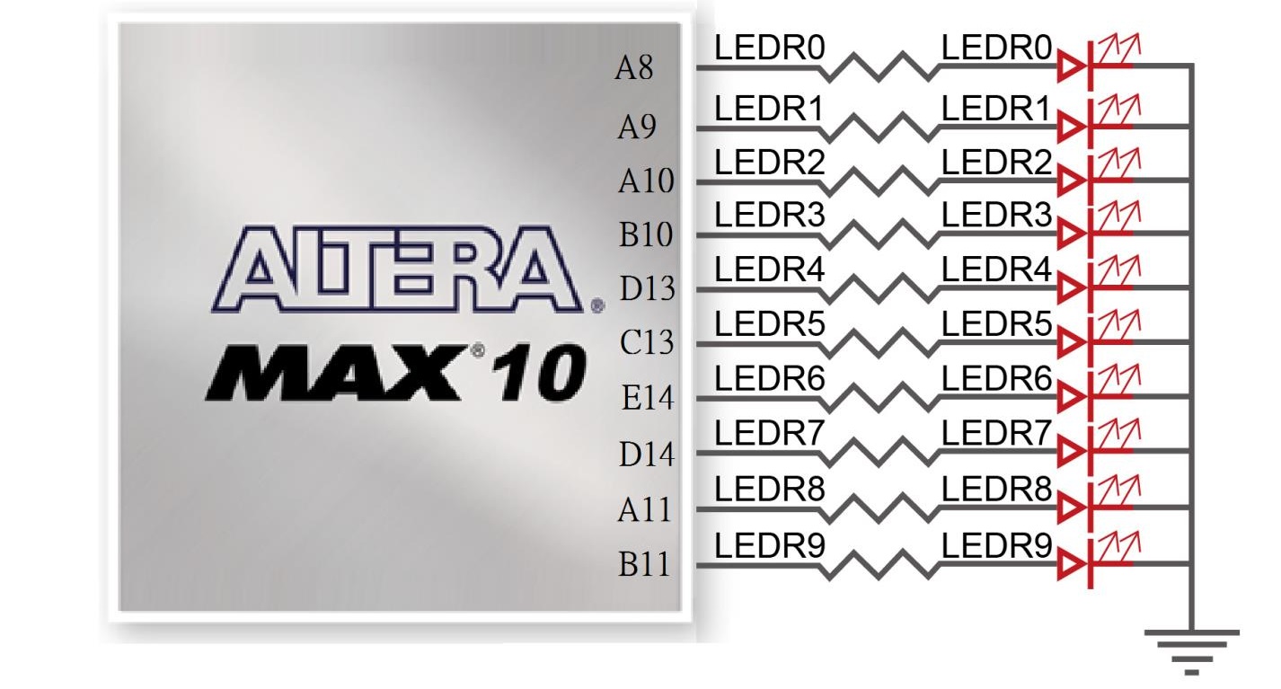
Figura 3.5 Conexión de los LEDs y la FPGA MAX 10
Signal Name |
FPGA Pin No. |
Description |
I/O Standard |
|---|---|---|---|
LEDR0 |
PIN_A8 |
LED [0] |
3.3-V LVTTL |
LEDR1 |
PIN_A9 |
LED [1] |
3.3-V LVTTL |
LEDR2 |
PIN_A10 |
LED [2] |
3.3-V LVTTL |
LEDR3 |
PIN_B10 |
LED [3] |
3.3-V LVTTL |
LEDR4 |
PIN_D13 |
LED [4] |
3.3-V LVTTL |
LEDR5 |
PIN_C13 |
LED [5] |
3.3-V LVTTL |
LEDR6 |
PIN_E14 |
LED [6] |
3.3-V LVTTL |
LEDR7 |
PIN_D14 |
LED [7] |
3.3-V LVTTL |
LEDR8 |
PIN_A11 |
LED [8] |
3.3-V LVTTL |
LEDR9 |
PIN_B11 |
LED [9] |
3.3-V LVTTL |
3.2.4. Usando los displays de 7-segmentos
La placa DE10-Lite tiene seis displays de 7 segmentos para mostrar números. La Figura 3.3 muestra la conexión de siete segmentos (ánodo común) a los pines de la MAX 10 FPGA. Cada segmento del display se puede activar o desactivar aplicando un nivel lógico bajo o un nivel lógico alto de la FPGA. Un nivel lógico alto lo apaga y un nivel lógico bajo lo enciende. Cada segmento de una pantalla está indexado de 0 a 6 y DP (punto decimal), con las posiciones correspondientes que se muestra en la Figura 3-17. La Tabla 3-6 muestra la asignación de pines de FPGA a las pantallas de 7 segmentos.
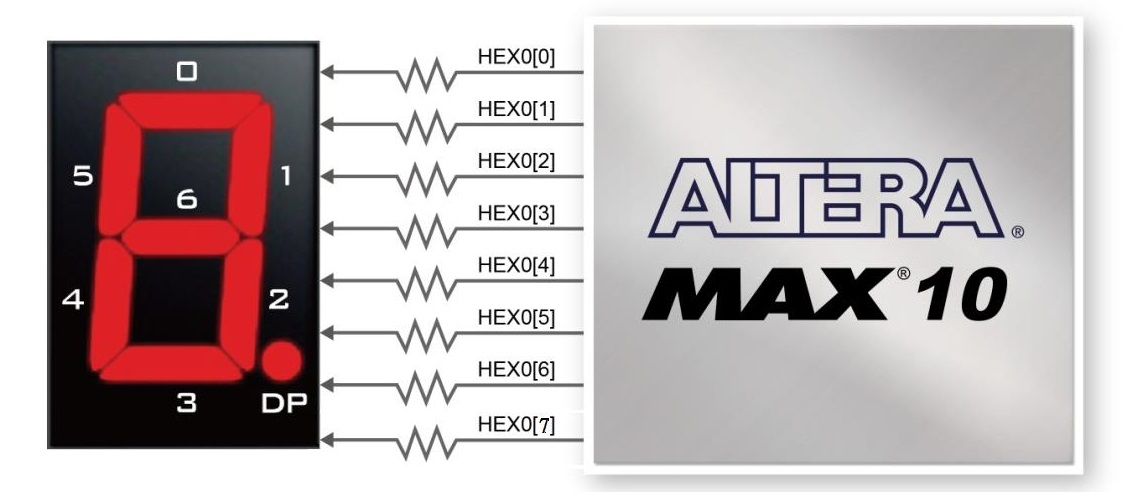
Figura 3.6 Conexión de los LEDs y la FPGA MAX 10
Signal Name |
FPGA Pin No. |
Description |
I/O Standard |
|---|---|---|---|
HEX00 |
PIN_C14 |
Seven Segment Digit 0[0] |
3.3-V LVTTL |
HEX01 |
PIN_E15 |
Seven Segment Digit 0[1] |
3.3-V LVTTL |
HEX02 |
PIN_C15 |
Seven Segment Digit 0[2] |
3.3-V LVTTL |
HEX03 |
PIN_C16 |
Seven Segment Digit 0[3] |
3.3-V LVTTL |
HEX04 |
PIN_E16 |
Seven Segment Digit 0[4] |
3.3-V LVTTL |
HEX05 |
PIN_D17 |
Seven Segment Digit 0[5] |
3.3-V LVTTL |
HEX06 |
PIN_C17 |
Seven Segment Digit 0[6] |
3.3-V LVTTL |
HEX07 |
PIN_D15 |
Seven Segment Digit 0[7], DP |
3.3-V LVTTL |
HEX10 |
PIN_C18 |
Seven Segment Digit 1[0] |
3.3-V LVTTL |
HEX11 |
PIN_D18 |
Seven Segment Digit 1[1] |
3.3-V LVTTL |
HEX12 |
PIN_E18 |
Seven Segment Digit 1[2] |
3.3-V LVTTL |
HEX13 |
PIN_B16 |
Seven Segment Digit 1[3] |
3.3-V LVTTL |
HEX14 |
PIN_A17 |
Seven Segment Digit 1[4] |
3.3-V LVTTL |
HEX15 |
PIN_A18 |
Seven Segment Digit 1[5] |
3.3-V LVTTL |
HEX16 |
PIN_B17 |
Seven Segment Digit 1[6] |
3.3-V LVTTL |
HEX17 |
PIN_A16 |
Seven Segment Digit 1[7], DP |
3.3-V LVTTL |
HEX20 |
PIN_B20 |
Seven Segment Digit 2[0] |
3.3-V LVTTL |
HEX21 |
PIN_A20 |
Seven Segment Digit 2[1] |
3.3-V LVTTL |
HEX22 |
PIN_B19 |
Seven Segment Digit 2[2] |
3.3-V LVTTL |
HEX23 |
PIN_A21 |
Seven Segment Digit 2[3] |
3.3-V LVTTL |
HEX24 |
PIN_B21 |
Seven Segment Digit 2[4] |
3.3-V LVTTL |
HEX25 |
PIN_C22 |
Seven Segment Digit 2[5] |
3.3-V LVTTL |
HEX26 |
PIN_B22 |
Seven Segment Digit 2[6] |
3.3-V LVTTL |
HEX27 |
PIN_A19 |
Seven Segment Digit 2[7], DP |
3.3-V LVTTL |
HEX30 |
PIN_F21 |
Seven Segment Digit 3[0] |
3.3-V LVTTL |
HEX31 |
PIN_E22 |
Seven Segment Digit 3[1] |
3.3-V LVTTL |
HEX32 |
PIN_E21 |
Seven Segment Digit 3[2] |
3.3-V LVTTL |
HEX33 |
PIN_C19 |
Seven Segment Digit 3[3] |
3.3-V LVTTL |
HEX34 |
PIN_C20 |
Seven Segment Digit 3[4] |
3.3-V LVTTL |
HEX35 |
PIN_D19 |
Seven Segment Digit 3[5] |
3.3-V LVTTL |
HEX36 |
PIN_E17 |
Seven Segment Digit 3[6] |
3.3-V LVTTL |
HEX37 |
PIN_D22 |
Seven Segment Digit 3[7], DP |
3.3-V LVTTL |
HEX40 |
PIN_F18 |
Seven Segment Digit 4[0] |
3.3-V LVTTL |
HEX41 |
PIN_E20 |
Seven Segment Digit 4[1] |
3.3-V LVTTL |
HEX42 |
PIN_E19 |
Seven Segment Digit 4[2] |
3.3-V LVTTL |
HEX43 |
PIN_J18 |
Seven Segment Digit 4[3] |
3.3-V LVTTL |
HEX44 |
PIN_H19 |
Seven Segment Digit 4[4] |
3.3-V LVTTL |
HEX45 |
PIN_F19 |
Seven Segment Digit 4[5] |
3.3-V LVTTL |
HEX46 |
PIN_F20 |
Seven Segment Digit 4[6] |
3.3-V LVTTL |
HEX47 |
PIN_F17 |
Seven Segment Digit 4[7], DP |
3.3-V LVTTL |
HEX50 |
PIN_J20 |
Seven Segment Digit 5[0] |
3.3-V LVTTL |
HEX51 |
PIN_K20 |
Seven Segment Digit 5[1] |
3.3-V LVTTL |
HEX52 |
PIN_L18 |
Seven Segment Digit 5[2] |
3.3-V LVTTL |
HEX53 |
PIN_N18 |
Seven Segment Digit 5[3] |
3.3-V LVTTL |
HEX54 |
PIN_M20 |
Seven Segment Digit 5[4] |
3.3-V LVTTL |
HEX55 |
PIN_N19 |
Seven Segment Digit 5[5] |
3.3-V LVTTL |
HEX56 |
PIN_N20 |
Seven Segment Digit 5[6] |
3.3-V LVTTL |
HEX57 |
PIN_L19 |
Seven Segment Digit 5[7], DP |
3.3-V LVTTL |