- SIR
- STH
- SFP
- SEP
- SIH
Network Infrastructure Service
The Network Infrastructure Service (SIR) of IUMA is responsible for defining, configuring, commissioning, and maintaining the computer system of the Institute.
The R&D&I activity of IUMA requires a significant computing, storage, and virtualization infrastructure that responds to the continuous demand for resources, both hardware and software, by researchers who develop internal projects or in collaboration with other entities.
There is its own data center with integrated connectivity in the ULPGC Gigabit network, whose resources are accessible from researchers' workstations and internal laboratories. Likewise, connectivity from the outside is possible through a secure remote access system.
The Service promotes the use of OpenSource applications for its operation, although it is also combined with proprietary systems and applications where it is necessary to maintain a high degree of resource availability as well as high levels of security required in a network with this degree of complexity.
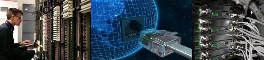
The main services under the responsibility of SIR are as follows:
- Network storage system.
- Virtualization system.
- Multi-platform authentication system.
- Computing systems.
- Remote access system with dual-factor authentication and encryption.
- Email with its own DNS domain.
- System of internal and external web services: internal management applications, webmail, official websites of the Institute, research project websites, personal websites of researchers, etc.
- Private storage cloud for secure resource sharing both internally and on the Internet.
- Gitlab-based version control system.
- Support service
Service of Technologies and Design Tools
Background
The task of implementing, supporting, and continuously improving the design infrastructure has been carried out since the creation of the Center for Applied Microelectronics (CMA) in 1990 and later the Institute of Applied Microelectronics (IUMA), with its participation in different actions:
- Special Action in Microelectronics (Microelectronics Workshop) of the National Microelectronics Program.
- EUROPCHIP Network of the European Union.
- EUROPRACTICE Network.
Competences
The Service of Technologies and Tools (STH) is created to coordinate access to IUMA's microelectronic design tools, as well as to coordinate the use of electronic systems manufacturing technologies. For this purpose, operations such as installation and support of design tools, training courses, fabrication of different integrated circuits, etc., are carried out.
- Competence on IUMA's design technologies and tools, both common and project-specific.
- Support to users in the development of electronic design activities.
- User support in accessing prototype and/or small-volume manufacturing technologies.
IUMA Objectives
- Evaluate, acquire, install, and maintain EDA software.
- Select, explore, and prepare design flows.
- Provide support and consultations to users within the service's capabilities.
- Report bugs and troubleshoot.
- Prepare documentation, manuals, and other support materials.
- Provide training and training for initial tool usage.
- Support for practices and course projects for teachers within specific agreements with the departments involved.
- Cooperate on research projects.
- Conduct continuous training activities.
- Provide the interface with manufacturers and technology suppliers.
- Acquire and install design kits and cell libraries from different manufacturers and technologies.
- Have contact with international support services.
- Assist in the completion of ICs and send them for manufacturing.
- Document different experiences.
- Disseminate activities through the service's website.
Available design tools
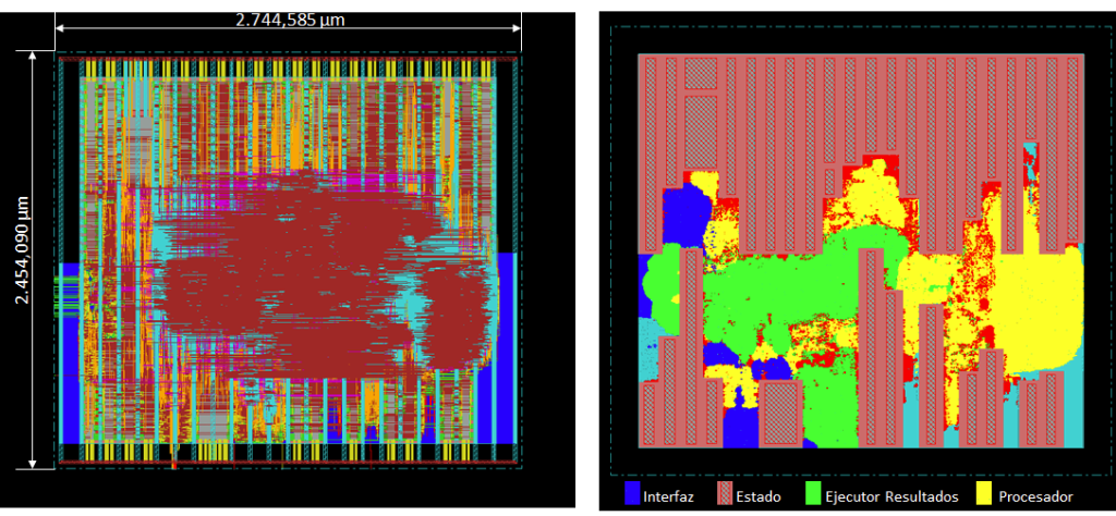
Currently, there is access to microelectronic design environments from Cadence, Siemens Mentor Graphics EDA, Synopsys, Intel FPGA, Xilinx FPGA, and Keysight ADS. With these environments, it is possible to perform the entire design flow, from specification, modeling, simulation, synthesis, layout implementation, advanced encapsulation design, to PCB design. Application domains include the design of analog, digital mixed-signal, RFIC, MEMS, SmartPower systems, and, in general, chip electronic systems (SoC).
Access to manufacturing
IUMA has access to various integrated circuit factories by being integrated into the EUROPRACTICE network. This allows the prototyping of designs in an initial experience for SMEs and also access to the manufacturing of small series. Examples of technologies include advanced 16nm CMOS nodes or low-cost 0.35-micron nodes, technologies for MEMS manufacturing, or integration of photonic devices with Silicon.
Service Manager: Dr. Pedro Pérez Carballo,
Manufacturing and Prototyping Service for Circuits
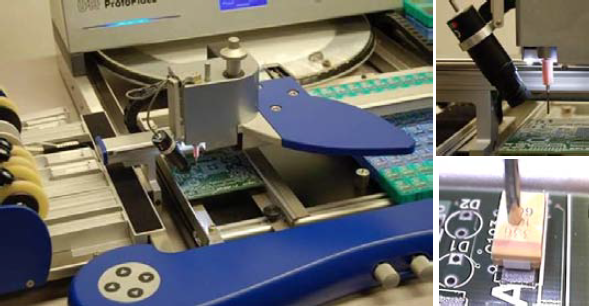
The "Service for Manufacturing Prototypes of Printed Circuits and Electronic Systems" has a modern laboratory for the prototyping of electronic systems, allowing the manufacturing of printed circuits with 2, 4, 6, and 8 layers in a few hours with a high level of quality, as well as the assembly, soldering, and testing of these circuits.
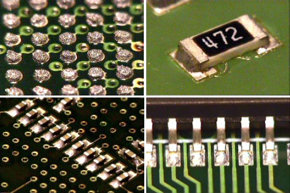
The equipment used allows obtaining the demanding levels of quality required for current electronic design. Designed for the prototyping and small-scale production of printed circuits, it also incorporates the possibility of machining aluminum panels and other materials, allowing the design and assembly of electromechanical systems.
Available services
- Manufacturing of simple and double-sided non-metalized printed circuits.
- Manufacturing of double-sided metalized printed circuits.
- Manufacturing of 4, 6, or 8-layer multicapade printed circuits.
- Manufacturing of special printed circuits (flexible substrates, RF, etc.).
- Assembly and soldering of prototypes and small series of printed circuits with insertion components, standard SMD. Fine-pitch and BGA SMD.
- Manufacturing of masks for solder paste dispensing.
- Manufacturing of high-precision phototools.
- Cleaning of printed circuits by ultrasound.
- Optical inspection of electronic circuits.
- Manufacturing of tip beds for small series electrical testing.
- Machining and labeling of aluminum panels for electronic systems.
- Design and assembly of electromechanical systems with structured aluminum.
Assembly and soldering of components
Se dispone de un sistema semiautomático de montaje de componentes SMD válido para todos los componentes existentes en el mercado, desde el footprint 0201. Se incluye también el servicio de montaje de componentes BGA, CSP y FlipChip, así como componentes fine-pich y ultra fine-pitch mediante estación de posicionamiento de hasta 50μm de precisión.
Paste soldering is done using reflow ovens that apply the required temperature profile. All equipment and materials used are prepared to work with the new European RoHS regulations that eliminate lead and other contaminating substances from production processes.
Small series testing
By manufacturing tip beds, the service offers testing for small series of circuits to its clients.
Cleaning and optical inspection
All manufactured circuits undergo an ultrasound cleaning procedure that ensures the removal of residues from the soldering process. Subsequently, an optical inspection with a microscope is carried out to verify the correct soldering of the components.
Tip Station Service
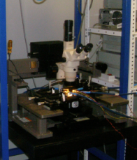
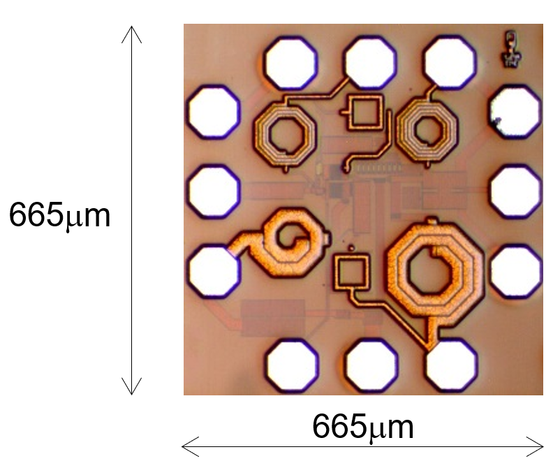
Over the past few years, IUMA has established a series of Common Services of the Institute for the use of resources that can be more intensively shared or have a more horizontal structure among the different divisions. Among them is the Tip Station Service (SEP) with competence focused on the large installation of the Tip Station for measuring integrated circuits on the wafer.
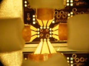
Precise measurement of circuits on the wafer is a fundamental task in the production of high-quality integrated circuits for applications in sectors such as communications, electronics, security imaging, radio astronomy, medical and health technologies, etc.
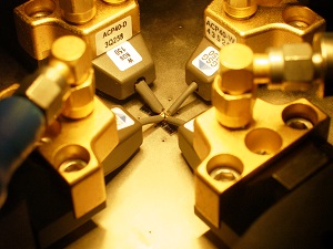
Scattering parameters, or S-parameters, are used to characterize electrical devices, especially when measuring the frequency and amplitude of the wave, rather than the current and voltage. Knowing the losses in amplitude and phase of transmitted and reflected signals is essential for the characterization of integrated circuits. This type of measurement poses a challenge, especially when the frequencies of the signals are very high, such as those used in current communication systems, such as the fifth generation of mobile communications (5G), satellite communications like Direct Broadcast Satellite (DBS), Satcom On the Move, Antennas for Gateways for mega-constellations of satellites, etc.
Through its Tip Station Service (SEP), IUMA provides support for the measurement of integrated circuits on the wafer not only to the research groups of the institute itself but also to academic and industrial groups nationally and internationally with which the institute is linked. This allows us to actively participate in a wide range of collaborative research projects on state-of-the-art applications.
Among the available material resources in the laboratory of the Tip Station Service, the following can be mentioned:
- Analytical Probe Station SUMMIT 9000 from Cascade Microtech
- S-parameter meter, Performance Network Analyzer (PNA) N5225B 10 MHz to 50 GHz
- Agilent Spectrum Analyzer, PSA Series Spectrum Analyzer, E4440A, 3Hz-26.5GHz
- Agilent Vector Signal Generator, ESG Vector Signal Generator, E4438C
- HB16 Thermosonic 90° Wedge & Ball & Bump Bonder micro-welding machine
- Semiconductor Device Analyzer B1500A
- Impedance Analyzer E4990A
- Additional instrumentation for conducting measurements
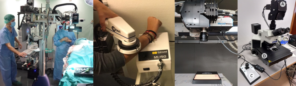
Hyperspectral Imaging Service
The Institute of Applied Microelectronics (IUMA) has the necessary means and resources, available to the research group, for conducting research using advanced hyperspectral imaging techniques. The main noteworthy resources related to this topic are as follows:
- Intraoperative hyperspectral imaging system for in-vivo brain tissue
- Hyperspectral dermatological imaging system
- Microscopic hyperspectral imaging acquisition system
- Macroscopic hyperspectral imaging acquisition systems in the laboratory
- Hyperspectral imaging capture system based on snapscan technology
- Hyperspectral imaging capture systems based on LCTF technology
- High-performance computing system based on Tesla K40 GPUS
- Liebherr biological sample freezer
- Other resources related to the research line: Ultimaker 3D Extended 3D printer. Used for the development of various hyperspectral imaging acquisition systems and part development.